
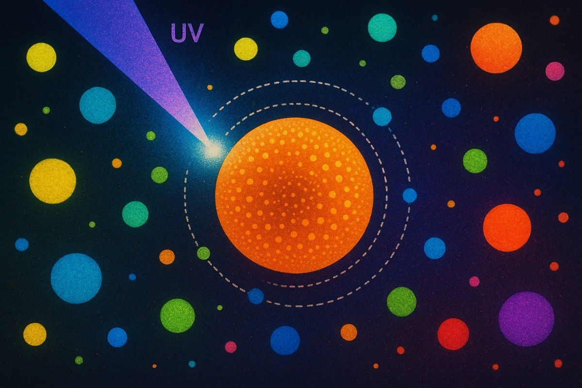
Quantum dots (QDs) are man-made nanoscale crystals that exhibit unique optical and electronic properties, including the ability to transport electrons and emit light of various colors when exposed to UV light. These artificially synthesized semiconductor nanoparticles have a wide range of potential applications, including use in composites, solar cells, fluorescent biological labeling, displays, lighting, and medical imaging.
Quantum dots nanoparticles of semiconductors were first theorized in the 1970s and then successfully synthesized in the early 1980s. When semiconductor particles are made small enough, they exhibit quantum effects, which restrict the energies at which electrons and holes (the absence of electrons) can exist within the particle. As energy is linked to wavelength (or color), this results in the optical properties of the particle being tunable based on its size. By controlling the size of the particle, it can be made to emit or absorb specific wavelengths (colors) of light.

Quantum dots are nanoscale man-made crystals that have the ability to convert a spectrum of light into different colors. Each dot emits a different color depending on its size. (Image: RNGS Reuters/Nanosys)
Quantum dots are artificial nanostructures that can possess many varied properties, depending on their material and shape. For instance, due to their particular electronic properties they can be used as active materials in single-electron transistors.
The properties of quantum dots (QDs) are determined by various factors, including size, shape, composition, and structure, such as whether they are solid or hollow. To utilize QDs effectively across multiple applications, including catalysis, electronics, photonics, information storage, imaging, medicine, and sensing, a dependable manufacturing technology is needed that can consistently produce large quantities of nanocrystals with uniform parameters. This will ensure that each batch of QDs has consistent and predictable properties for a given application.
Because certain biological molecules are capable of molecular recognition and self-assembly, nanocrystals could also become an important building block for self-assembled functional nanodevices.
The atom-like energy states of QDs furthermore contribute to special optical properties, such as a particle-size dependent wavelength of fluorescence; an effect which is used in fabricating optical probes for biological and medical imaging.
The use of colloidal quantum dots in bioanalytics and biolabeling has emerged as one of the most promising areas of application for these artificial nanoscale crystals. Despite the early potential demonstrated by the first generation of quantum dots, significant efforts were required to improve basic properties, particularly the colloidal stability of these particles in salt-containing solutions.
Initially, quantum dots were only used in controlled laboratory conditions and would not have been practical for use in real-world samples such as blood. However, these stability issues have since been resolved, allowing for the widespread use of quantum dots in real-world applications.

Vials of quantum dots producing vivid colors. For instance, a cadmium-based quantum dot showing pure, highly specific green color response. (Image: NASA)
Quantum dots have found applications in composites, solar cells (Grätzel cells) and fluorescent biological labels (for example to trace a biological molecule) which use both the small particle size and tunable energy levels.
Advances in chemistry have resulted in the preparation of monolayer-protected, high-quality, monodispersed, crystalline quantum dots as small as 2 nm in diameter, which can be conveniently treated and processed as a typical chemical reagent.
Quantum dots in medicine
Quantum dots enable researchers to study cell processes at the level of a single molecule and may significantly improve the diagnosis and treatment of diseases such as cancers. QDs are either used as active sensor elements in high-resolution cellular imaging, where the fluorescence properties of the quantum dots are changed upon reaction with the analyze, or in passive label probes where selective receptor molecules such as antibodies have been conjugated to the surface of the dots.
Quantum dots could revolutionize medicine. Unfortunately, most of them are toxic. Ironically, the existence of heavy metals in QDs such as cadmium, a well-established human toxicant and carcinogen, poses potential dangers especially for future medical application, where q dots are deliberately injected into the body.
As the use of nanomaterials for biomedical applications is increasing, environmental pollution and toxicity have to be addressed, and the development of a non-toxic and biocompatible nanomaterial is becoming an important issue.
Quantum dots in photovoltaic
The attractiveness of using quantum dots for making solar cells lies in several advantages over other approaches: They can be manufactured in an energy-saving room-temperature process; they can be made from abundant, inexpensive materials that do not require extensive purification, as silicon does; and they can be applied to a variety of inexpensive and even flexible substrate materials, such as lightweight plastics.
Although using quantum dots as the basis for solar cells is not a new idea, attempts to make photovoltaic devices have not yet achieved sufficiently high efficiency in converting sunlight to power.
A promising route for quantum dot solar cells is a semiconductor ink with the goal of enabling the coating of large areas of solar cell substrates in a single deposition step and thereby eliminating tens of deposition steps necessary with the previous layer-by-layer method.
Graphene quantum dots
Graphene, which basically is an unrolled, planar form of a carbon nanotube therefore, has become an extremely interesting candidate material for nanoscale electronics. Researchers have shown that it is possible to carve out nanoscale transistors from a single graphene crystal (i.e. graphene quantum dots). Unlike all other known materials, graphene remains highly stable and conductive even when it is cut into devices one nanometer wide.

Quantum dot carved from a graphene sheet. (Image: Mesoscopic Physics Group, University of Manchester)
Graphene quantum dots (GQDs) also show great potential in the fields of photoelectronics, photovoltaics, biosensing, and bioimaging owing to their unique photoluminescence (PL) properties, including excellent biocompatibility, low toxicity, and high stability against photobleaching and photoblinking.Scientists still are working on finding efficient and universal methods for the synthesis of GQDs with high stability, controllable surface properties, and tunable PL emission wavelength.
Perovskite quantum dots
Luminescent quantum dots (LQDs), which possess high photoluminescence quantum yields, flexible emission color controlling, and solution processibility, are promising for applications in lighting systems (warm white light without UV and infrared irradiation) and high quality displays.
However, the commercialization of LQDs has been held back by the prohibitively high cost of their production. Currently, LQDs are prepared by the HI method, requiring at high temperature and tedious surface treating in order to improve both optical properties and stability.
Although developed only recently, inorganic halide perovskite quantum dot systems have exhibited comparable and even better performances than traditional QDs in many fields.
By preparing highly emissive inorganic perovskite quantum dots (IPQDs) at room temperature, IPQDs’ superior optical merits could lead to promising applications in lighting and displays.
Quantum dot TVs and displays
The most commonly known use of quantum dots nowadays may be TV screens. Samsung and LG launched their QLED TVs in 2015, and a few other companies followed not long after.
Quantum dots, because they are both photo-active (photoluminescent) and electro-active (electroluminescent) and have unique physical properties, will be at the core of next-generation displays. Compared to organic luminescent materials used in organic light emitting diodes (OLEDs), QD-based materials have purer colors, longer lifetime, lower manufacturing cost, and lower power consumption. Another key advantage is that, because QDs can be deposited on virtually any substrate, you can expect printable and flexible even rollable quantum dot displays of all sizes.
Quantum Dots in Quantum Information Processing
A quantum dot is the structure on a semiconductor that is able to confine electrons in three dimensions such that discrete energy levels are obtained. The quantum dot behaves as an artificial atom, whose properties can be controlled. Quantum dots can be formed spontaneously by depositing a semiconductor material on a substrate with different lattice spacing (this configuration is known as a heterostructure). The quantum dots have a bowl-like shape with a diameter ∼100 nm and height ∼30 nm, as illustrated in Fig. 13.26. The layer of AlGaAs of ∼5 nm thickness is placed between two thicker layers of GaAs. The lower GaAs layer is n doped to provide free electrons at the upper GaAs–AlGaAs interface, forming a so-called2D) “electron gas”.
This process of formation of 2D electron gas is equivalent to total internal reflection, as two interface layers serve as boundaries of layers with different refractive indices. Furthermore, an array of metal contacts (gates) is placed on the top of the upper GaAs layer (50–10 nm above the 2D electron gas). External voltages are applied on these gates to restrict movement of the electrons in the horizontal plane. 3D potential wells are induced in the region among metal electrodes.
There are many different schemes that can be used by employing this concept. One approach is based on electron–hole pairs, also known as excitons, whose energy is given by Eexcitons = Ebg – Ebe, where Ebg is the band-gap energy and Ebe is the binding energy of electron–hole pairs. Now by using two quantum dots, the entangled qubits can be formed. The electron and hole can be in the first dot, representing the state |0〉, or in the second dot, representing the state |1〉.
Let the first qubit correspond to the electron and the second qubit correspond to the hole. The state |00〉 denotes that the electron–hole pair is located in the first dot, while the |11〉 state denotes that the electron–hole pair is located in the second dot. The state |01〉 denotes that the electron is in the first dot and the hole is in the second dot. Finally, the state |10〉 denotes that the hole is in the first dot and the electron is in the second dot. By providing that the distance between two interacting dots is ∼5 nm, the electron and holes can tunnel from one dot to the other dot.
– Dr. Mamataben Soni, Associate Professor
FOBAS, Madhav University